Modbus protocol overview
- Modbus is a serial fieldbus protocol, a de-facto standard for industrial devices. This page summarizes the protocol.
Introduction
- Modbus is an application-layer fieldbus. It is independent of the physical medium and runs over RS-232, RS-422, RS-485, TCP/IP, and more.
- Common framing modes include Modbus ASCII, Modbus RTU, and Modbus TCP.
- On serial links you choose RTU or ASCII. RTU is compact binary with a CRC; ASCII encodes each byte as two ASCII characters and uses an LRC checksum.
- On Ethernet, Modbus TCP wraps the PDU without the serial CRC (integrity is handled by TCP/IP).
- Modbus is master–slave and request/response. Slaves respond to the master. Only one master request is in flight at a time: master transmit → slave reply; if the master is silent, the bus is idle.
ADU and PDU
A complete Modbus frame is an Application Data Unit (ADU) that wraps a Protocol Data Unit (PDU) independent of the physical layer.

The figure shows the ADU/PDU relationship. A complete Modbus RTU ADU looks like:
<---------   ADU   ---------->
01  05  00  00  FF  00  DD  FA
    <----  PDU   ---->
Frame = slave address (1 B) + function code (1 B) + data (N B) + checksum (2 B).
| Name | Role |
|---|---|
| Slave address | Target slave (1–247) |
| Function code | Operation (e.g. read coils / read holding regs) |
| Data | Parameters (start address, quantity, …) |
| Checksum | Error detection (CRC / LRC) |
01: Slave address
05: FC 0x05 — write single coil
00 00 FF 00: PDU — coil address 0x0000, value 0xFF00 (ON)
DD FA: CRC (example bytes)
This example writes coil 1 ON for slave 0x01. The following PDU discussion omits the serial CRC (ADU-specific).
The typical transaction is shown below: the master (client) sends a request; the slave (server) executes and replies, or returns an exception if an error occurs; the master interprets responses to verify success or failure.
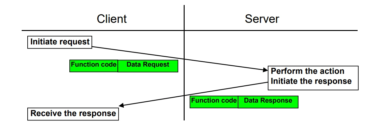
Modbus transaction (no error)
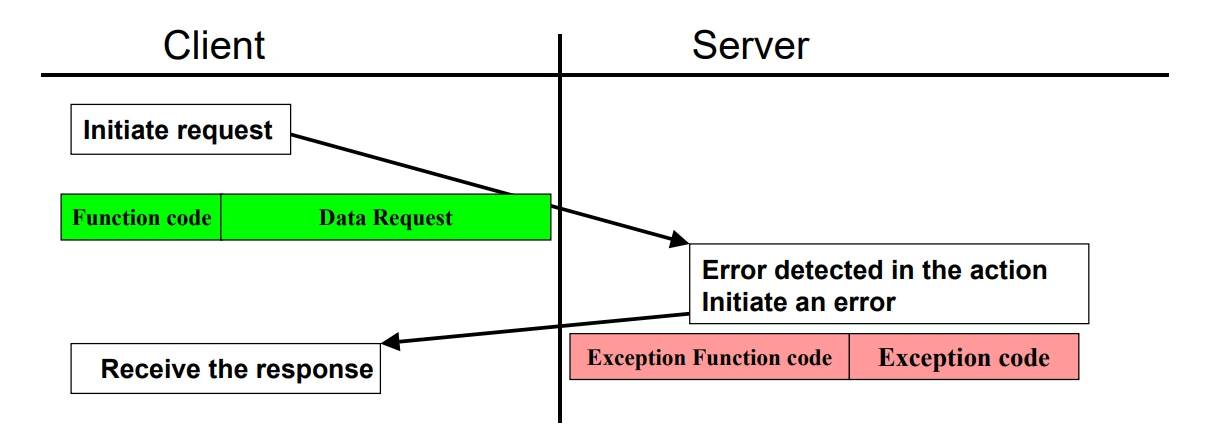
Modbus transaction (exception response)
For request 05 00 00 FF 00, a normal response echoes the same PDU bytes; an illegal-data case might return 85 03. Below is the full RTU ADU (address + PDU + CRC).
Request: 01 05 00 00 FF 00 8C 3A
Normal response: 01 05 00 00 FF 00 8C 3A
Exception response: 01 85 03 02 91
Normal response: response FC equals request FC.
Exception response: exception FC = request FC + 0x80.
Exception codes are one byte. Common codes:
| Code | Name | Description |
|---|---|---|
| 0x01 | Illegal function | Function not supported |
| 0x02 | Illegal data address | Invalid data address |
| 0x03 | Illegal data value | Invalid data value or operation |
| 0x04 | Server failure | Server device failure |
| 0x05 | Acknowledge | Acknowledged; processing |
| 0x06 | Device busy | Slave is busy and cannot execute |
The diagram below illustrates server-side handling: receive → validate FC (exception 0x01 if invalid) → validate address (exception 0x02 if invalid) → validate data value (exception 0x03 if invalid) → execute (exceptions 0x04, 0x05, or 0x06 on failure) → return normal response.
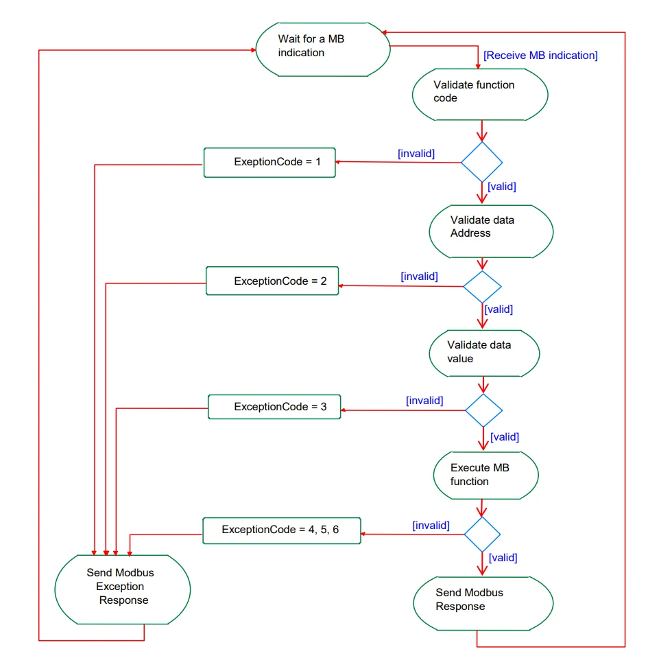
Modbus transaction state diagram
Data types
Modbus defines four primary tables, often denoted 0x, 1x, 3x, and 4x.
| Table | Range | Data type | Access | FC | Typical use |
|---|---|---|---|---|---|
| Coils | 0x0000–0xFFFF | Bit (1 bit) | R/W | 01h, 05h, 0Fh | Relays / DO |
| Discrete inputs | 1x0000–1xFFFF | Bit (1 bit) | R | 02h | Buttons / switches |
| Input registers | 3x0000–3xFFFF | Word (16 bit) | R | 04h | Sensors / analog inputs |
| Holding registers | 4x0000–4xFFFF | Word (16 bit) | R/W | 03h, 06h, 10h | Setpoints / analog outputs |
Note: PLC addressing often uses 5-digit forms (e.g. 40001). On the wire registers are 0-based, so PLC address = protocol address + 1.
0x = coils (DO), 1x = discrete inputs (DI), 3x = input registers (AI), 4x = holding registers (AO).
Each table is independent; use the matching FCs to access each type.
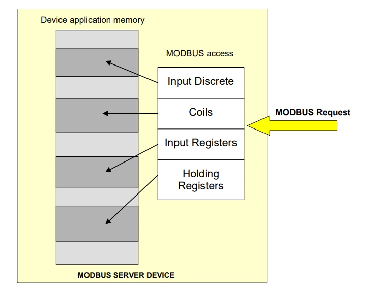
Modbus data model
Function codes
Many function codes exist; the table below lists the most common read/write operations.
| FC | Description |
|---|---|
| 01 | Read coils |
| 02 | Read discrete inputs |
| 03 | Read holding registers |
| 04 | Read input registers |
| 05 | Write single coil |
| 06 | Write single register |
| 0F | Write multiple coils |
| 10 | Write multiple registers |
0x01 Read coils
This FC reads 1–2000 consecutive coils. The request supplies the start address (first coil) and quantity.
Coil numbering is zero-based (human “coil 1” → address 0).
- Request
| FC | 1 byte | 0x01 |
|---|---|---|
| Start address | 2 bytes | 0x0000 ~ 0xFFFF |
| Quantity | 2 bytes | 1 ~ 2000(0x7D0) |
- Response
Coils are packed one bit per coil; 1 = ON, 0 = OFF.
The first data byte’s LSB is the first addressed output; further bits follow within the byte, then the next bytes, LSB-first.
If the coil count is not a multiple of 8, the final byte is zero-padded toward the MSB. The byte count field states how many data bytes follow.
| FC | 1 byte | 0x01 |
|---|---|---|
| Byte count | 1 byte | N* |
| Coil data | N bytes | n = N or N+1 |
*N = ceil(coil_count / 8)
- Exception
| Exception FC | 1 byte | 0x81 |
|---|---|---|
| Exception code | 1 byte | 01, 02, 03, 04 |
- Example
This example reads coils 20 through 38.
Request: 01 01 00 13 00 13 8C 02
01: Slave address
01: FC 0x01 (read coils)
00 13: Start address (hex 0x0013 = 19, +1 human numbering = coil 20)
00 13: Quantity (19 coils = coil 20 through 38)
8C 02: CRC
Response: 01 01 03 CD 6B 05 42 82
01: Slave address
01: FC 0x01 (read coils)
03: Byte count (19 coils = 3 bytes: 2 full bytes + 3 bits + 5 padding bits)
CD: Coils 27–20 (1100 1101)
6B: Coils 35–28 (0110 1011)
05: Coils 38–36 (0000 0101)
42 82: CRC
Pad the five unused MSBs of the last byte with 0.
0x02 Read discrete inputs
This FC reads 1–2000 consecutive discrete inputs. The request supplies the start address and quantity.
Discrete inputs are zero-based (human “input 1” → address 0).
- Request
| FC | 1 byte | 0x02 |
|---|---|---|
| Start address | 2 bytes | 0x0000 ~ 0xFFFF |
| Quantity | 2 bytes | 1~2000(0x7D0) |
Discrete inputs are packed one bit per input; 1 = ON, 0 = OFF.
The first data byte’s LSB is the first addressed input; remaining bits follow in the same packing order.
If the input count is not a multiple of 8, the final byte is zero-padded toward the MSB. The byte-count field states the number of complete data bytes.
- Response
| FC | 1 byte | 0x02 |
|---|---|---|
| Byte count | 1 byte | N* |
| Input data | N bytes | n = N or N+1 |
*N = ceil(input_count / 8)
- Exception
| Exception FC | 1 byte | 0x82 |
|---|---|---|
| Exception code | 1 byte | 01, 02, 03, 04 |
- Example
This example reads discrete inputs 197 through 218.
Request:01 02 00 C4 00 16 B8 39
01: Slave address
02: FC 0x02 (read discrete inputs)
00 C4: Start address (hex 0x00C4 = 196, +1 human numbering = input 197)
00 16: Quantity (22 bits = inputs 197 through 218)
B8 39: CRC
Response: 01 02 03 AC DB 35 22 88
01: Slave address
02: FC 0x02 (read discrete inputs)
03: Byte count (22 bits = 3 bytes: 2 bytes + 6 bits + 2 padding bits)
AC: Discrete inputs 204–197 (1010 1100)
DB: Discrete inputs 212–205 (1101 1011)
35: Discrete inputs 218–213 (0011 0101)
22 88: CRC
Pad the two unused MSBs of the last byte with 0.
0x03 Read holding registers
This FC reads a contiguous block of holding registers. The request specifies the starting register address and quantity.
Holding registers are zero-based (human “register 1” → address 0).
- Request
| FC | 1 byte | 0x03 |
|---|---|---|
| Start address | 2 bytes | 0x0000 ~ 0xFFFF |
| Quantity | 2 bytes | 1~125(0x7D) |
Register data is packed as two bytes per register (high byte first, then low byte).
- Response
| FC | 1 byte | 0x03 |
|---|---|---|
| Byte count | 1 byte | 2×N* |
| Register data | N×2 bytes |
*N = register count
- Exception
| Exception FC | 1 byte | 0x83 |
|---|---|---|
| Exception code | 1 byte | 01, 02, 03, 04 |
- Example
This example reads registers 108 through 110. Each register is 16 bits (two bytes).
Request:01 03 00 6B 00 03 74 17
01: Slave address
03: FC 0x03 (read holding registers)
00 6B: Start address (hex 0x006B = 107, +1 human numbering = register 108)
00 03: Quantity (read 3 registers 108–110)
74 17: CRC
Response: 01 03 06 02 2B 00 00 00 64 05 7A
01: Slave address
03: FC 0x03 (read holding registers)
06: Byte count (3 registers × 2 bytes each = 6 bytes)
02 2B: Register 108 (Hi/Lo)
00 00: Register 109 (Hi/Lo)
00 64: Register 110 (Hi/Lo)
05 7A: CRC
0x04 Read input registers
This FC reads 1–125 consecutive input registers. The request specifies start register and count.
Input registers are zero-based.
- Request
| FC | 1 byte | 0x04 |
|---|---|---|
| Start address | 2 bytes | 0x0000–0xFFFF |
| Quantity | 2 bytes | 1–125 (0x7D) |
Input register data is packed as two bytes per register (high byte first, then low byte).
- Response
| FC | 1 byte | 0x04 |
|---|---|---|
| Byte count | 1 byte | 2×N* |
| Input register values | N×2 bytes |
*N = Number of input registers
- Exception
| Exception FC | 1 byte | 0x84 |
|---|---|---|
| Exception code | 1 byte | 01, 02, 03, 04 |
- Example
This example reads input register 9.
Request: 01 04 00 08 00 01 B0 08
01: Slave address
04: FC 0x04 (read input registers)
00 08: Start address (hex 0x0008 = 8, +1 human numbering = input register 9)
00 01: Quantity (read 1 register)
B0 08: CRC
Response: 01 04 02 00 0A 39 37
01: Slave address
04: FC 0x04 (read input registers)
02: Byte count (1 register × 2 bytes = 2 bytes)
00 0A: Register 9 data
39 37: CRC
0x05 Write single coil
This FC writes a single coil ON or OFF. The data field carries the requested state. The PDU addresses the target coil.
Coil addresses are zero-based.
Payload 0xFF00 requests ON; 0x0000 requests OFF. Any other value is illegal and must not change the coil.
- Request
| FC | 1 byte | 0x05 |
|---|---|---|
| Coil address | 2 bytes | 0x0000–0xFFFF |
| Value | 2 bytes | 0x0000 or 0xFF00 |
- Response
| FC | 1 byte | 0x05 |
|---|---|---|
| Coil address | 2 bytes | 0x0000–0xFFFF |
| Value | 2 bytes | 0x0000 or 0xFF00 |
- Exception
| Exception FC | 1 byte | 0x85 |
|---|---|---|
| Exception code | 1 byte | 01, 02, 03, 04 |
- Example
This example turns coil 173 ON.
Request: 01 05 00 AC FF 00 4C 1B
01: Slave address
05: FC 0x05 (write single coil)
00 AC: Coil address (hex 0x00AC = 172, +1 human numbering = coil 173)
FF 00: Value to write (**0xFF00** = ON, **0x0000** = OFF)
4C 1B: CRC
Response: 01 05 00 AC FF 00 4C 1B
01: Slave address
05: FC 0x05 (write single coil)
00 AC: Coil address (hex 0x00AC = 172, +1 human numbering = coil 173)
FF 00: Value to write (**0xFF00** = ON, **0x0000** = OFF)
4C 1B: CRC
0x06 Write single register
This FC writes one holding register. The request carries address and value.
Register addresses are zero-based.
- Request
| FC | 1 byte | 0x06 |
|---|---|---|
| Register address | 2 bytes | 0x0000–0xFFFF |
| Register value | 2 bytes | 0x0000–0xFFFF |
- Response
| FC | 1 byte | 0x06 |
|---|---|---|
| Register address | 2 bytes | 0x0000–0xFFFF |
| Register value | 2 bytes | 0x0000–0xFFFF |
- Exception
| Exception FC | 1 byte | 0x86 |
|---|---|---|
| Exception code | 1 byte | 01, 02, 03, 04 |
- Example
This example writes 0x0003 to register 2.
Request: 01 06 00 01 00 03 98 0B
01: Slave address
06: FC 0x06 (write single register)
00 01: Register address (hex 0x0001 = 1, +1 human numbering = register 2)
00 03: Value written (0x0003)
98 0B: CRC
Response: 01 06 00 01 00 03 98 0B
01: Slave address
06: FC 0x06 (write single register)
00 01: Register address (hex 0x0001 = 1, +1 human numbering = register 2)
00 03: Value written (0x0003)
98 0B: CRC
0x0F Write multiple coils
This FC forces each coil in a sequence ON or OFF; the request specifies start address, quantity, and coil states.
Coil addresses are zero-based.
Coil states are encoded in the data field: bit 1 requests ON, bit 0 requests OFF for each mapped coil.
- Request
| FC | 1 byte | 0x0F |
|---|---|---|
| Start address | 2 bytes | 0x0000–0xFFFF |
| Coil quantity | 2 bytes | 0x0001–0x07B0 |
| Byte count | 1 byte | N* |
| Output values | N×1 byte |
*N = ceil(output_count / 8)
- Response
| FC | 1 byte | 0x0F |
|---|---|---|
| Start address | 2 bytes | 0x0000 ~ 0xFFFF |
| Quantity | 2 bytes | 0x0001 ~ 0x07B0 |
- Exception
| Exception FC | 1 byte | 0x8F |
|---|---|---|
| Exception code | 1 byte | 01, 02, 03, 04 |
- Example
This example writes 10 coils starting at coil 20.
Request: 01 0F 00 13 00 0A 02 CD 01 72 CB
01: Slave address
0F: FC 0x0F (write multiple coils)
00 13: Start address (hex 0x0013 = 19, +1 human numbering = coil 20)
00 0A: Number of coils to write (hex 0x0A = 10)
02: Byte count (10 coils = 2 bytes: 1 byte + 2 bits + 6 padding bits)
CD: Coils 27–20 (1100 1101)
01: Coils 29–28 (0100 0001)
72 CB: CRC
Response: 01 0F 00 13 00 0A 24 09
01: Slave address
0F: FC 0x0F (write multiple coils)
00 13: Start address (hex 0x0013 = 19, +1 human numbering = coil 20)
00 0A: Number of coils to write (hex 0x0A = 10)
24 09: CRC
0x10 Write multiple registers
This FC writes 1–123 consecutive holding registers. The PDU contains start address, quantity, and data (two bytes per register).
- Request
| FC | 1 byte | 0x10 |
|---|---|---|
| Start address | 2 bytes | 0x0000–0xFFFF |
| Register quantity | 2 bytes | 0x0001–0x007B |
| Byte count | 1 byte | 2×N* |
| Register values | N×2 bytes |
*N = register count
- Response
| FC | 1 byte | 0x10 |
|---|---|---|
| Start address | 2 bytes | 0x0000–0xFFFF |
| Register quantity | 2 bytes | 0x0001–0x007B |
- Exception
| Exception FC | 1 byte | 0x90 |
|---|---|---|
| Exception code | 1 byte | 01, 02, 03, 04 |
- Example
This example writes 0x000A and 0x0102 to registers 2 and 3.
Request: 01 10 00 01 00 02 04 00 0A 01 02 92 30
01: Slave address
10: FC 0x10 (write multiple registers)
00 01: Start address (hex 0x0001 = 1, +1 human numbering = register 2)
00 02: Number of registers to write
04: Byte count (2 registers × 2 bytes each = 4 bytes)
00 0A: Value for register 2
01 02: Value for register 3
92 30: CRC
Response: 01 10 00 01 00 02 10 08
01: Slave address
10: FC 0x10 (write multiple registers)
00 01: Start address (hex 0x0001 = 1, +1 human numbering = register 2)
00 02: Number of registers to write
10 08: CRC
NewLink Modbus module registers
This section lists register usage for NewLink Modbus I/O modules.
Relay outputs
| Address (HEX) | Content | Values | Access | Modbus FC |
|---|---|---|---|---|
| 0x0000 … 0x0007 | CH1–CH8 relay coils | 0xFF00: relay ON; 0x0000: relay OFF | R/W | 0x01, 0x05, 0x0F |
The table above is the 8-channel relay coil map. 0x addresses are coils (DO); use FC 0x01, 0x05, or 0x0F.
- Read relay state
Request: 01 01 00 00 00 08 3D CC
01: Slave address
01: FC 0x01 (read coils)
00 00: Start address of relays to read
00 08: Number of relays to read
3D CC: CRC
- Control single relay
Request: 01 05 00 00 FF 00 8C 3A
01: Slave address
05: FC 0x05 (write single coil)
00 00: Relay address to operate
FF 00: Value to write
8C 3A: CRC
- Write relay states
Request: 01 0F 00 00 00 08 01 FF BE D5
01: Slave address
0F: FC 0x0F (write multiple coils)
00 00: Start address of relays to operate
00 08: Number of relays to write
01: State byte count
FF: Relay bitmask; each bit maps to one relay
BE D5: CRC
Discrete inputs
| Address (HEX) | Content | Values | Access | Modbus FC |
|---|---|---|---|---|
| 1x0000 … 1x0007 | CH1–CH8 discrete inputs | State of inputs CH1–CH8 | R | 0x02 |
The table above is the 8-channel discrete input map. 1x addresses are discrete inputs (DI); use FC 0x02.
- Read discrete inputs
Request: 01 02 00 00 00 08 79 CC
01: Slave address
02: FC 0x02 (read discrete inputs)
00 00: Start address of discrete inputs to read
00 08: Number of discrete inputs to read
79 CC: CRC
Analog inputs
| Address (HEX) | Content | Values | Access | Modbus FC |
|---|---|---|---|---|
| 3x0000 … 3x0007 | CH1–CH8 analog input data | Unsigned 16-bit values | R | 0x04 |
The table above is the 8-channel analog input map. 3x addresses are input registers (AI); use FC 0x04.
- Read analog inputs
Request: 01 04 00 00 00 08 F1 CC
01: Slave address
04: FC 0x04 (read input registers)
00 00: Start address of inputs to read
00 08: Input quantity to read
F1 CC: CRC
Analog outputs
| Address (HEX) | Content | Values | Access | Modbus FC |
|---|---|---|---|---|
| 4x0000 … 4x0007 | CH1–CH8 analog output data | Unsigned 16-bit values | R/W | 0x03, 0x06, 0x10 |
The table above is the 8-channel analog output map. 4x addresses are holding registers (AO); use FC 0x03, 0x06, or 0x10.
- Read holding registers (outputs)
Request: 01 03 00 00 00 08 44 0C
01: Slave address
03: FC 0x03 (read holding registers)
00 00: Start address of outputs to read
00 08: Output quantity to read
44 0C: CRC
- Write single analog output
Request: 01 06 00 00 03 E8 89 74
01: Slave address
06: FC 0x06 (write single register)
00 00: Output register address
03 E8: Data value
89 74: CRC
- Write multiple analog outputs
Request: 01 10 00 00 00 08 10 03 E8 03 E8 03 E8 03 E8 03 E8 03 E8 03 E8 03 E8 3C 05
01: Slave address
10: FC 0x10 (write multiple registers)
00 00: Start address of the first register
00 08: Number of registers to write
10: Output byte count
03 E8: CH1 analog output
…
03 E8: CH8 analog output
3C 05: CRC